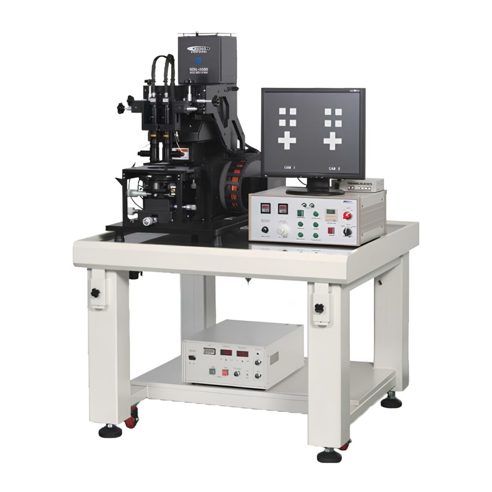
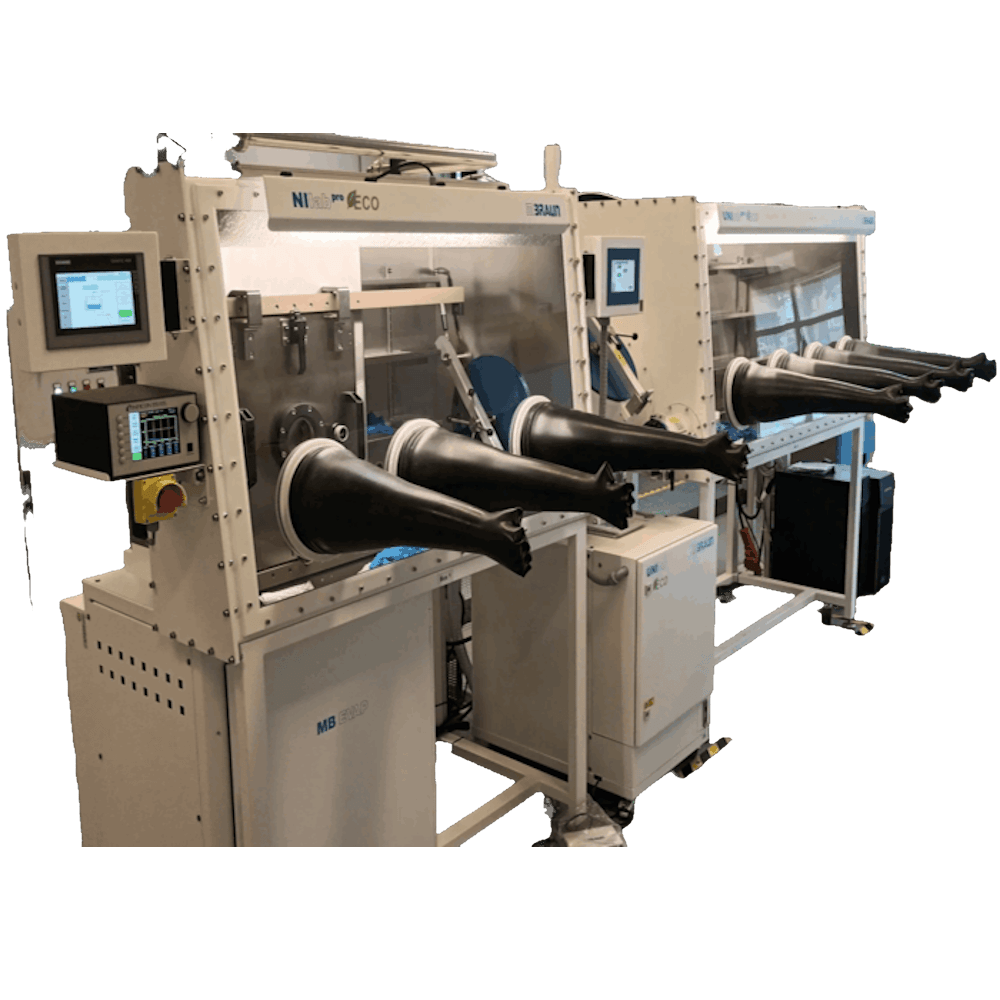
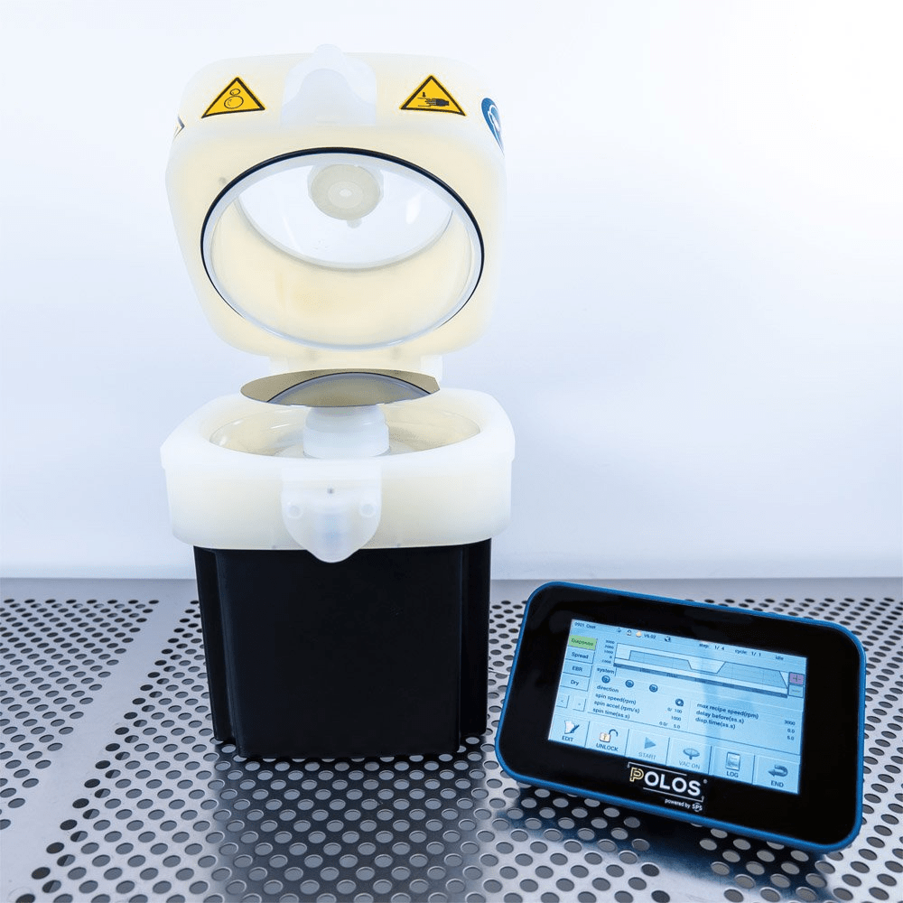
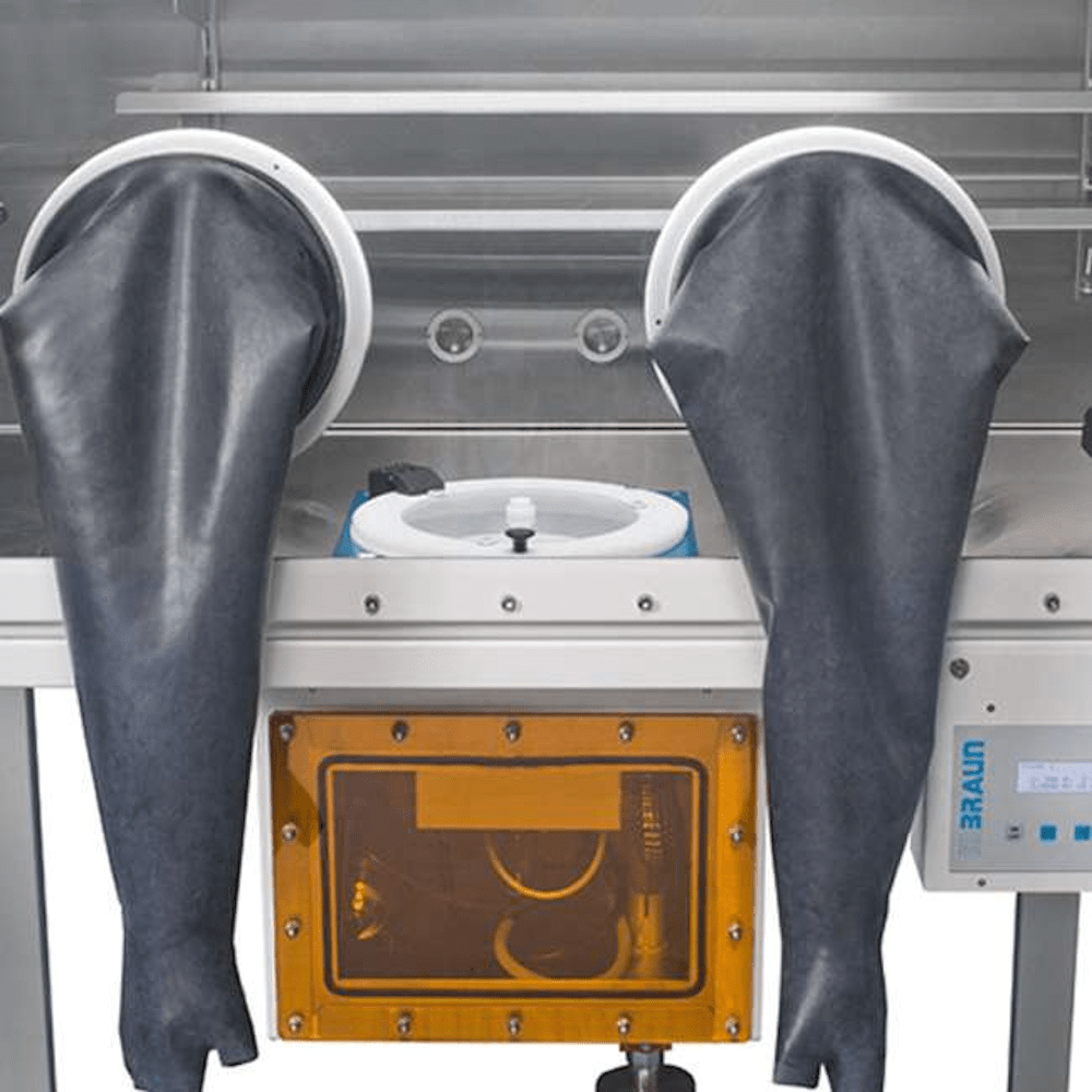
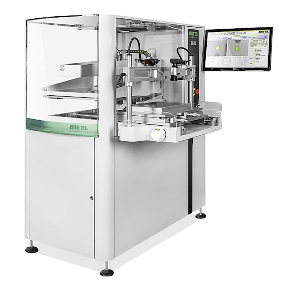
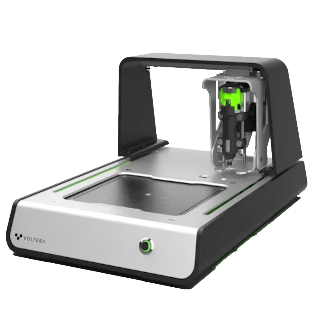
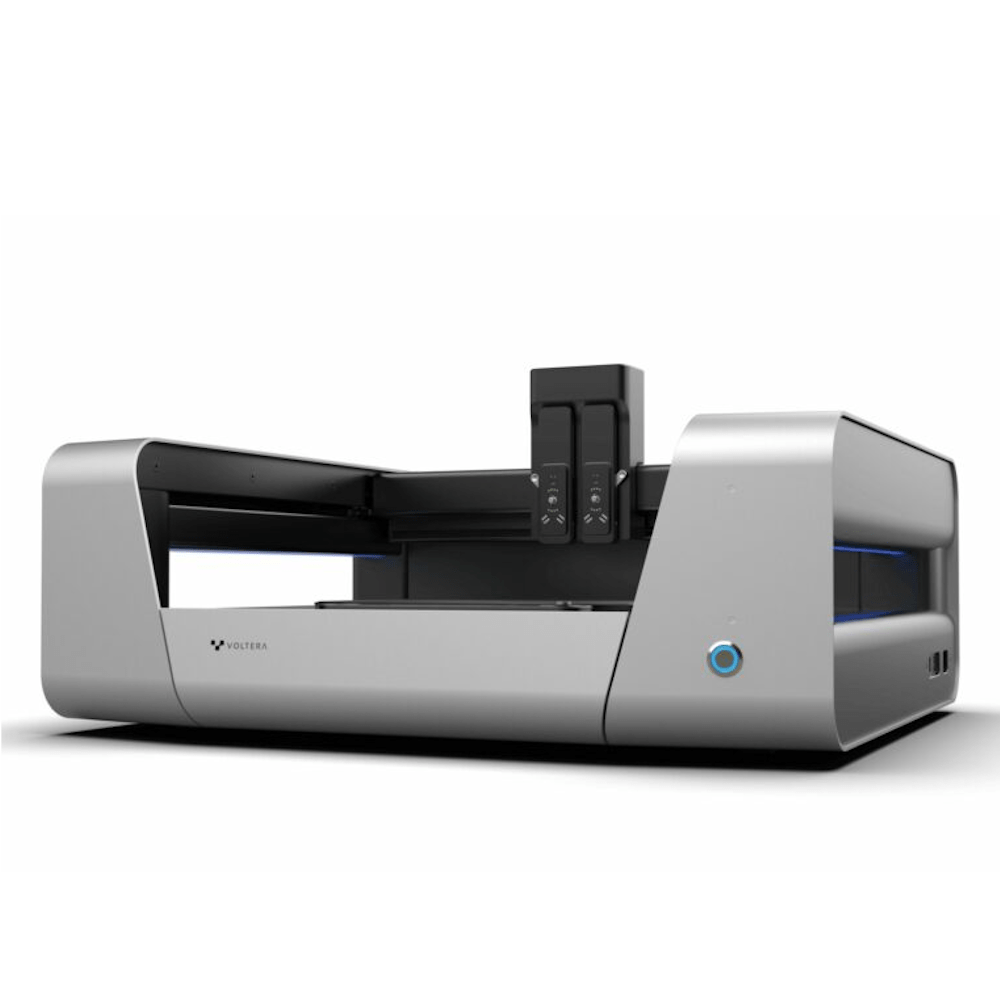
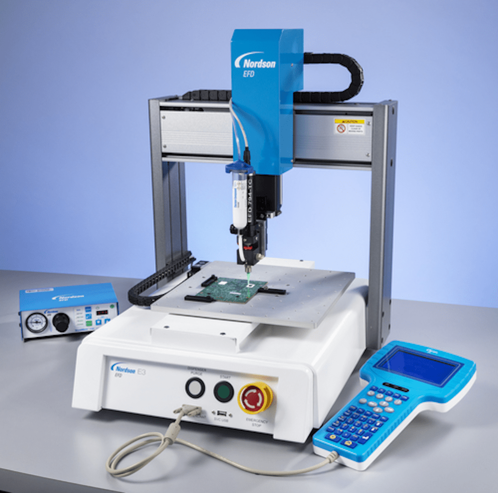
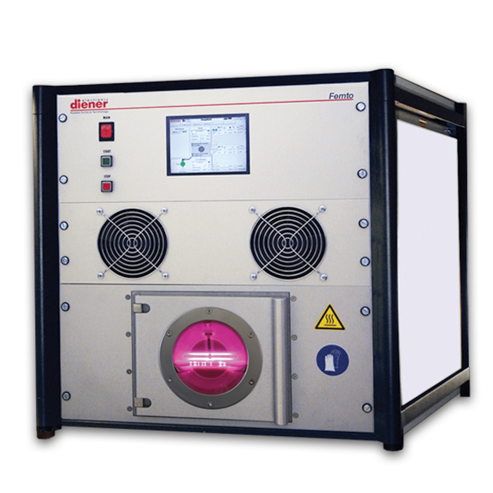
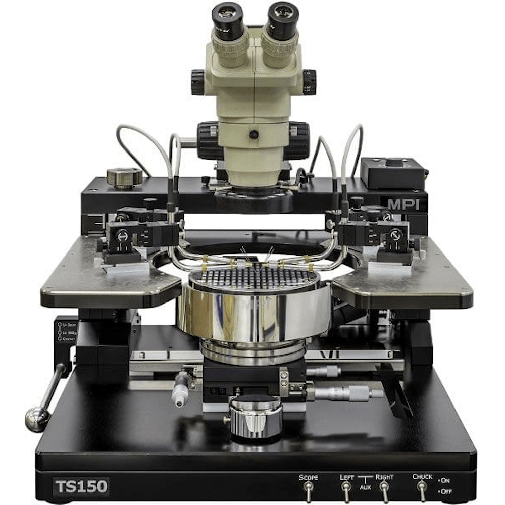
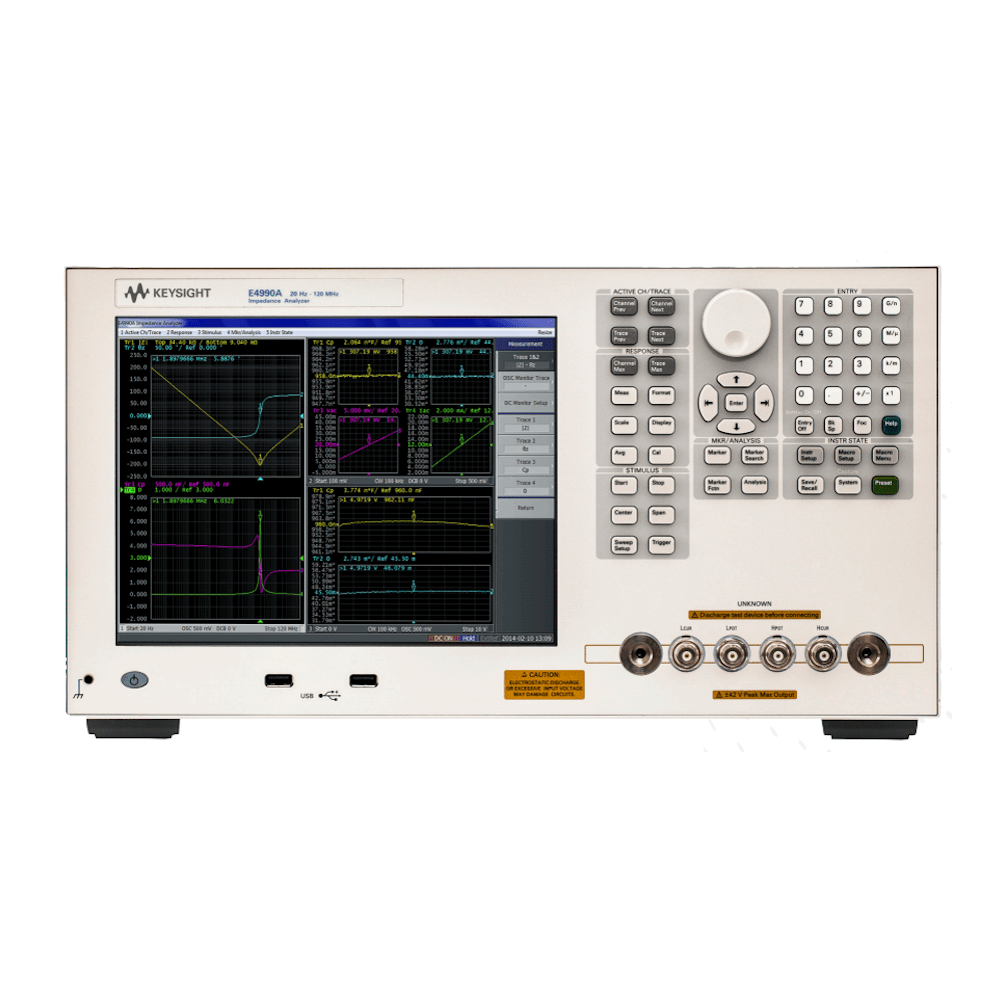
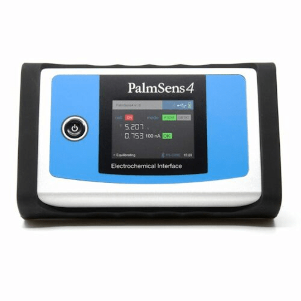
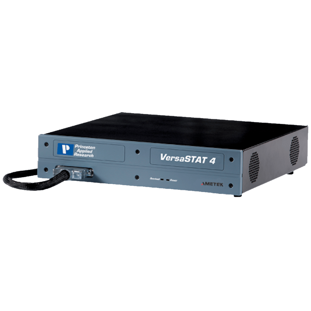
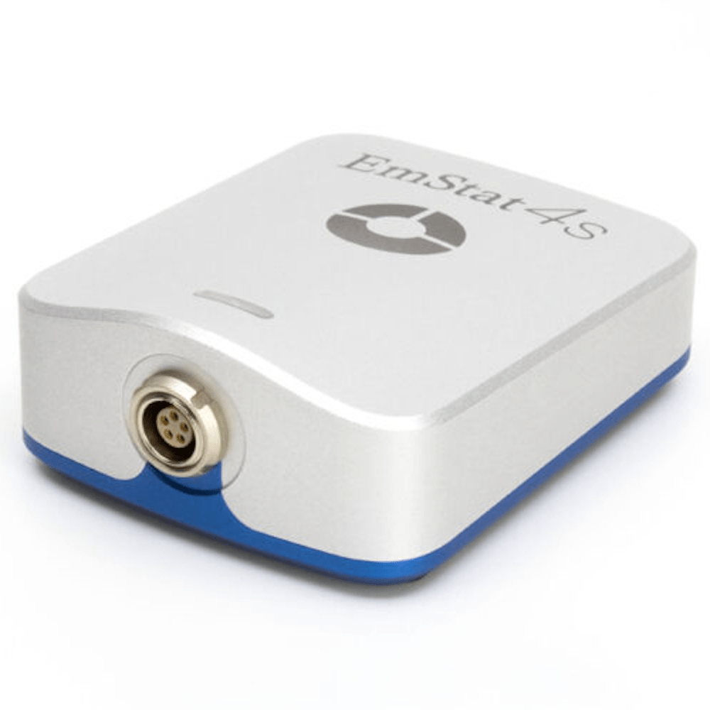
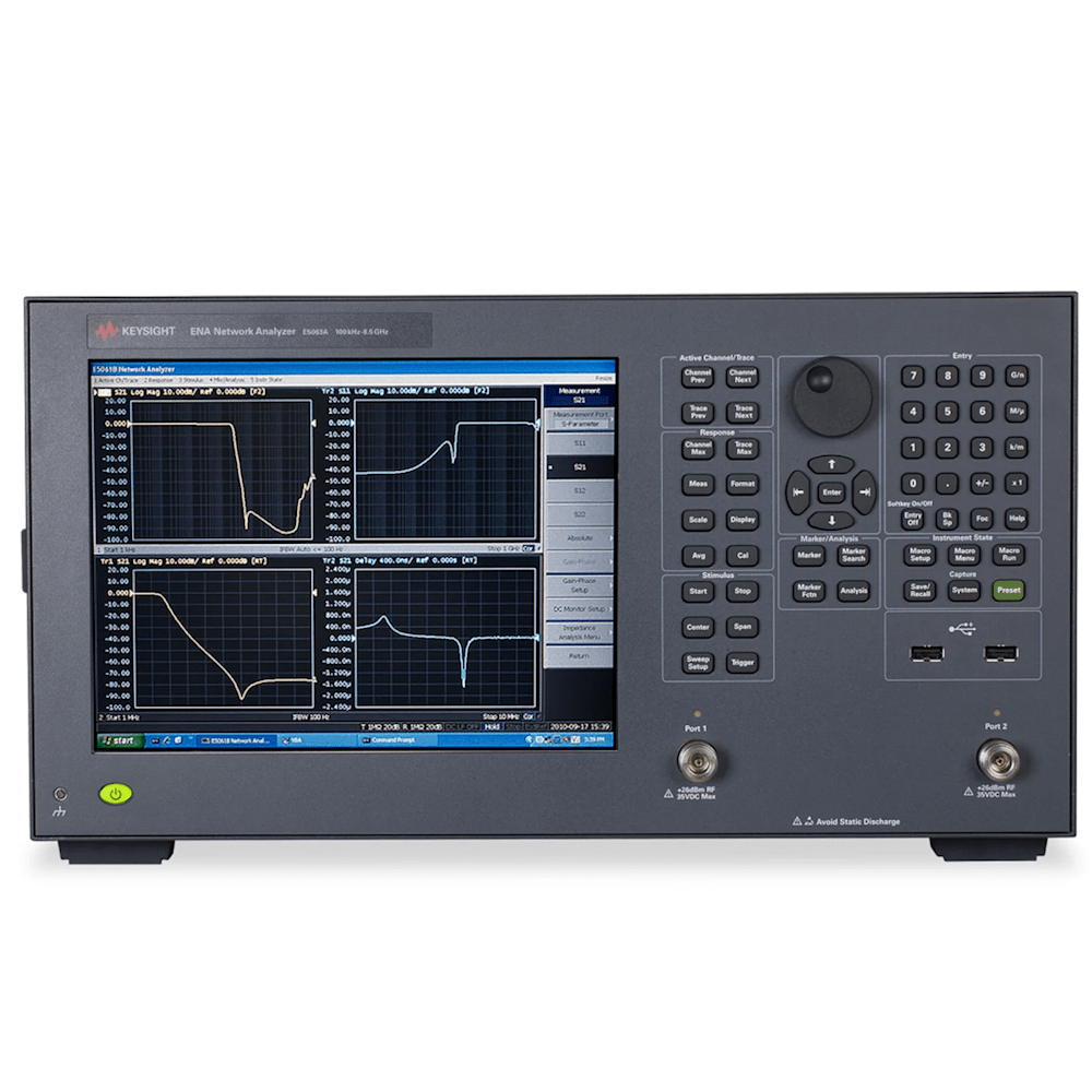
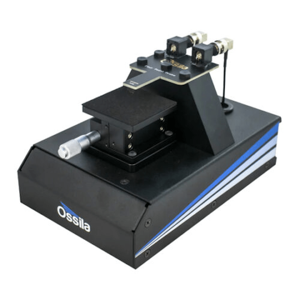
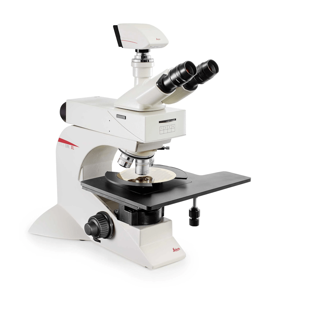
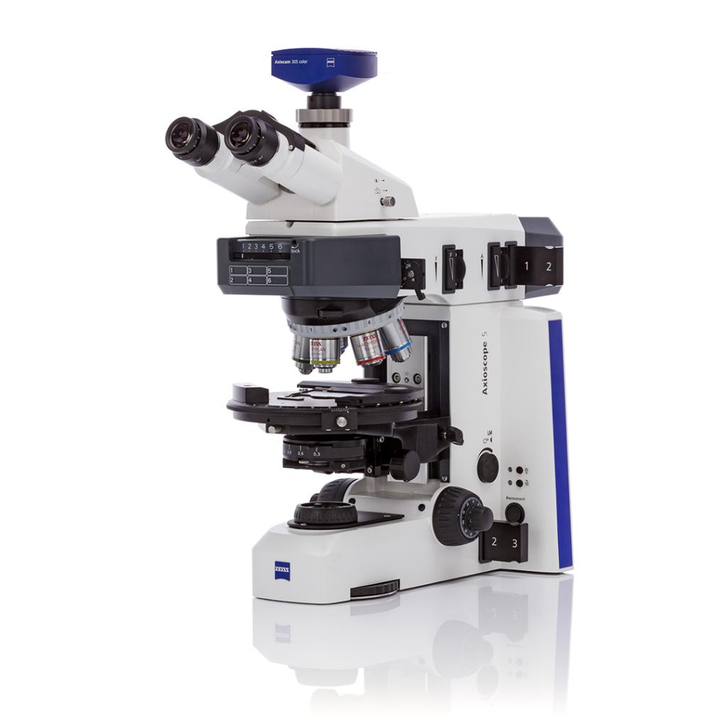
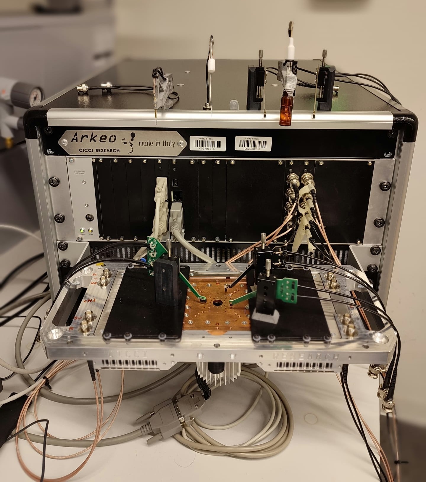
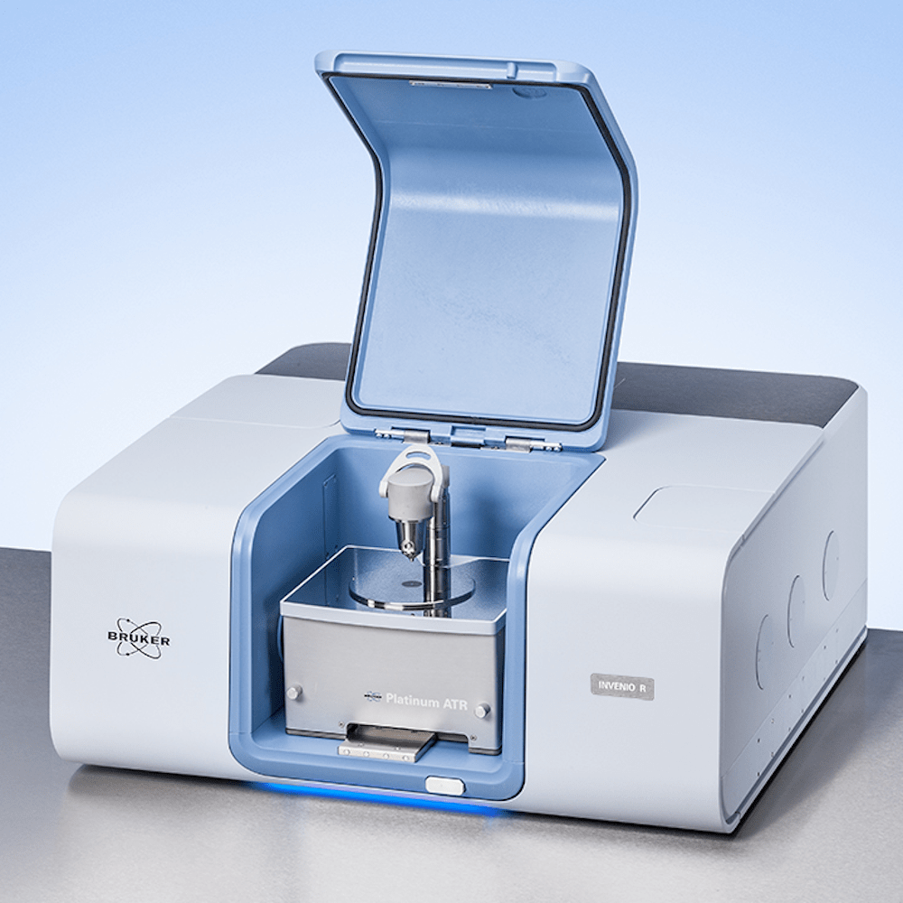
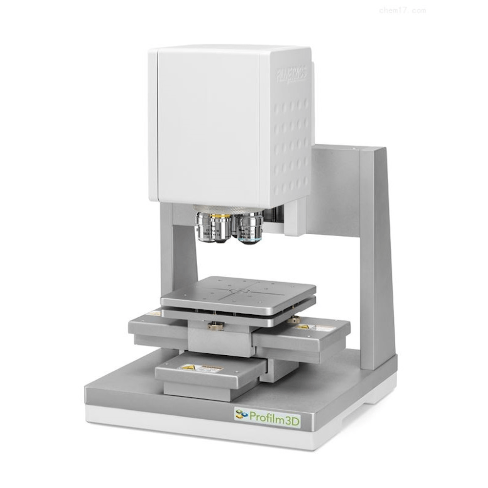
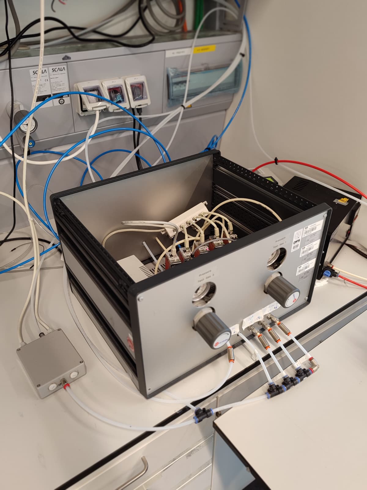
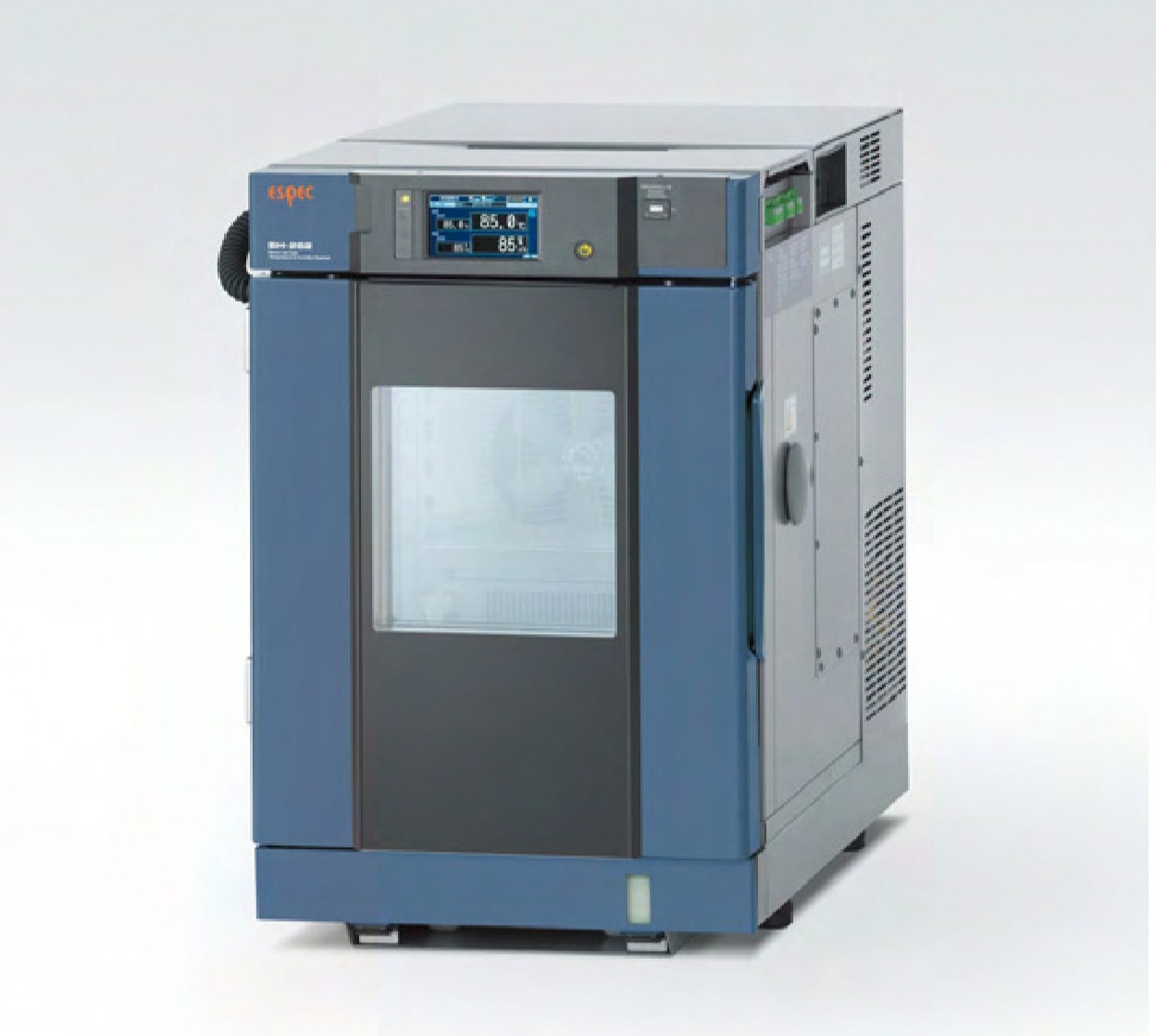
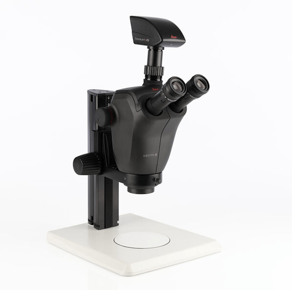
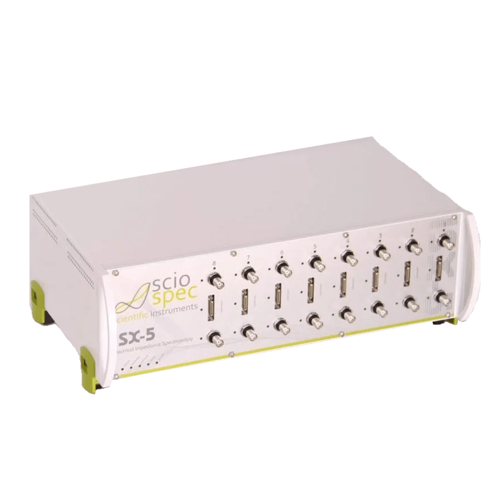
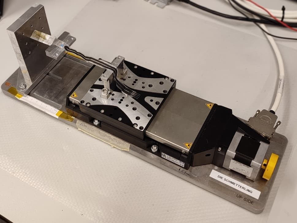
LAB EQUIPMENT FABRICATION Mask Aligner The MIDAS MDA-400M is a manual mask aligner that enables accurate alignment and UV exposure of photomasks onto substrates up to 4 inches, supporting high-resolution pattern transfer for microfabrication processes. Thermal & E-beam EvaporatorMBraun ProVap SmartBeam BeamTrek is a combined thermal and electron‑beam thin‑film deposition system that allows precise, high‑purity material evaporation onto substrates under high vacuum Spin CoaterPolos Spin 150X is a high‑performance spin coating system used in microfabrication to evenly apply photoresists and other liquid films onto substrates by controlled high‑speed rotation, ensuring uniform thin layers for lithography and surface processing. Spin CoaterMBraun MB‑SC‑210 is a precision spin coater designed for consistent, reproducible coating of photoresists and functional films in cleanroom and research environments. Screen PrinterAurel C920 Model is a precision screen printer used in electronics and microfabrication to deposit uniform patterns of solder paste, adhesives, or inks onto substrates, ensuring repeatable registration and high throughput. Dispense PrinterVoltera V‑One is a compact digital dispensing printer that deposits conductive inks and solder pastes directly onto circuit boards for rapid prototyping of printed electronics and simple PCB designs without traditional fabrication. Dispense PrinterVoltera NOVA is an advanced electronics dispensing system that prints high‑resolution conductive traces, dielectric inks, and solder paste, enabling rapid prototyping and functional circuitry fabrication with automated toolpaths and enhanced precision. Spray CoaterNordson EFD E4 is a professional spray coating system designed to apply uniform liquid films such as photoresists and specialty coatings over substrates, offering controlled atomization and consistent coverage for research or production environments. Plasma AsherDiener Femto is a plasma ashing system used for resist removal, surface cleaning, and surface activation in microfabrication for semiconductor and materials research. ELECTRICAL AND ELECTROCHEMICAL CHARACTERIZATION Probe StationMPI TS‑150 is a precision probe station for electrical testing of wafers and devices, offering micromanipulated contacts and stable positioning for characterization of semiconductor and microelectronic components. Impedence AnalyzerKeysight E4990A is a high‑performance impedance analyzer used to measure complex impedance, capacitance, and dielectric properties across a wide frequency range for materials, components, and circuits. PotentiostatPalmsens 4 is a potentiostat/galvanostat system for electrochemical measurements, commonly used in research on batteries, sensors, corrosion, and materials characterization. PotentiostatPrinceton Applied Research VersaSTAT 4 is a high‑end potentiostat/galvanostat offering advanced control for detailed analysis of electrochemical systems in research and development. PotentiostatEmStat 4s is a potentiostat/galvanostat platform designed for electrochemical testing and sensing applications with flexible connectivity and measurement options. Network AnalyzerKeysight E5061B is a professional vector network analyzer (VNA) for characterizing S‑parameters, impedance, and RF performance of components and systems over a broad frequency range. 4-point ProbeOssila 4‑point probe is a materials characterization tool for measuring the sheet resistance of thin films using a four‑terminal configuration to eliminate contact resistance errors. Optical MicroscopeLeica DM8000M is a high‑end optical research microscope providing brightfield and advanced imaging capabilities with versatile contrast methods for materials science and biological applications. Optical MicroscopeZeiss Axio is a modular optical microscope platform known for high‑resolution imaging and flexibility across contrast techniques, widely used in research, quality control, and life sciences. All‑in‑One Measurement PlatformArkeo by Cicci Research Srl is versatile research instrument (often used for nanoscale characterization or advanced microscopy), enabling high‑resolution imaging/analysis depending on the specific configuration. and application FT-IR SpectrometerBruker FT‑IR Spectrometer is used for identifying chemical bonds and molecular compositions via infrared absorption spectroscopy. Optical ProfilometerFilmetrics Optical Profilometer is a precision optical thickness and reflectance measurement tool used to characterize thin films and coatings with sub-nanometer accuracy. Gas ChamberA custom gas chamber is designed to simulate controlled atmospheric conditions by introducing specific gases at defined concentrations. It is used to test the performance, durability, and safety of materials or components when exposed to particular chemical environments under regulated temperature and pressure conditions. Climate ChamberThe Espec SH-262 temperature humidity chamber is a bench-top environmental chamber used to simulate controlled temperature and humidity conditions for testing materials and electronic components. It allows precise regulation of climate parameters to evaluate product performance, reliability, and durability under different environmental stresses. Contact Angle GoniometerOssila Contact Angle Goniometer is a precision contact angle measurement system used to quantify surface wettability, surface energy and liquid interactions on films and substrates. Optical 3D ProfilometerLeica Ivesta 3 is a high-resolution optical 3D profilometer for non-contact surface topography and thickness measurements in materials and semiconductor research Electrical Impedence SpectroscopeSciospec iSX‑5 is a high-performance electrical impedance spectroscope for broadband dielectric and impedance spectroscopy of materials, components and electrochemical systems. Stretching MachineConstructed at Unibz, this machine allows for ____
